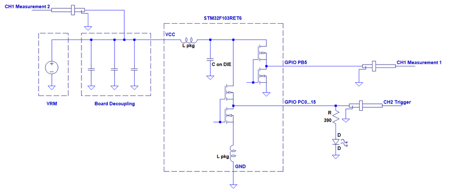
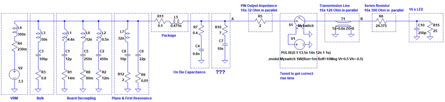
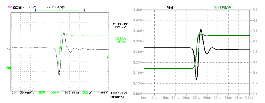
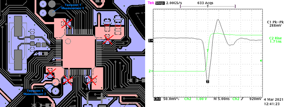
In this part, I want to show the noise voltage on VCC when the GPIOs of the STM32 uC are switching. To directly measure the voltage on the die of the chip, an additional GPIO is held at high level and the probe is connected to this GPIO.
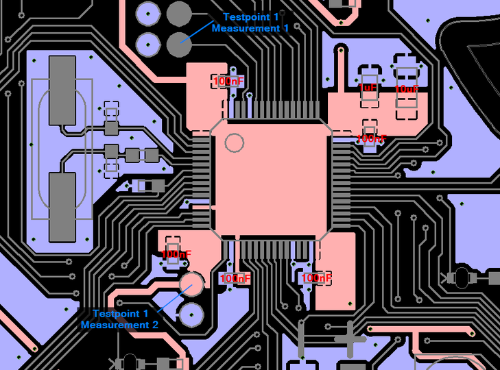
The layout shows the typically placed 100 nF caps on each PWR/GND pair of the uC with additional 1 uF and 10 uF caps.
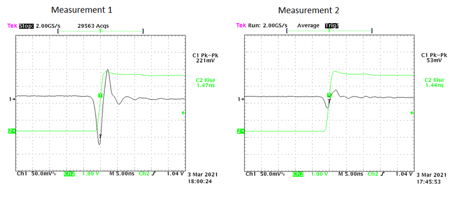
The measurement of the voltage on-die shows a peak to peak value of 221 mV. The voltage measured on the board itself shows a voltage of only 53 mVpp. This shows, that a large part of the voltage drop occurs in the package. This also means that the decoupling on the PCB is effective, and an even lower impedance will not bring lower noise levels directly on the chip.
The simulation model developed in Part 3 of this series shows the same result.
Next, the decoupling caps were removed one after the other.
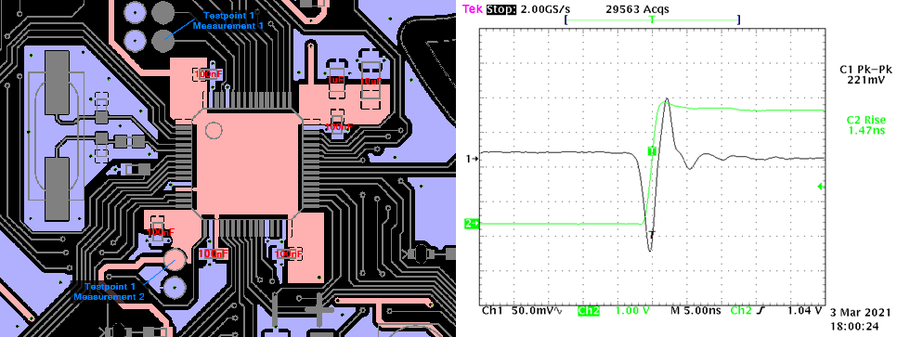
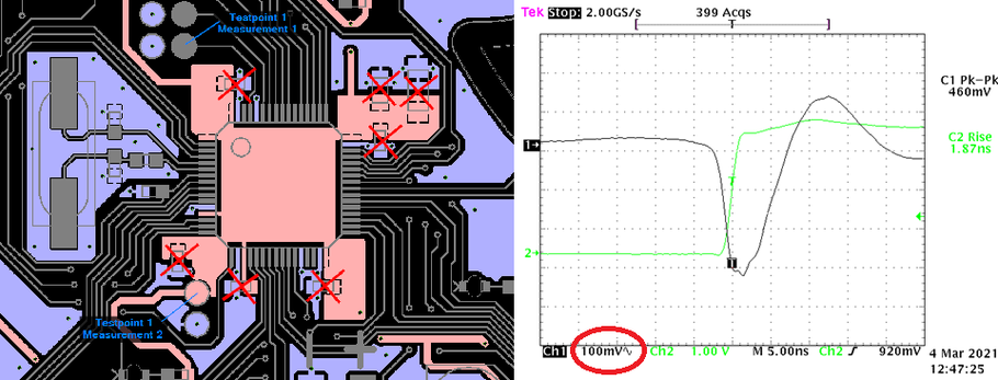
In the last case there was only a 10 uF KERKO at the Step down converter at a distance of about 30 mm. Now the voltages on-die and on the PCB testpoints match. This means that the voltage drop is caused by the excessive impedance of the supply system on the PCB and not by the inductivity of the package.
I conclude that following the datasheet recommendations and placing a 100 nf capacitor to each power pin will give very good results on a 2-layer board. I emphasize "to each power pin" because it does not make sense to place all 4 100 nF caps to one power pin. They have to be spatially distributed.
Write a comment