With my latest project, I wanted to check the noise generated by a buck converter on its input. The goal was to give some insights on how to lay out the input filter of a buck converter. Due to the principle of a buck converter there are fast transient currents on the input side. A decoupling capacitor connected with low additional inductance is mandatory.
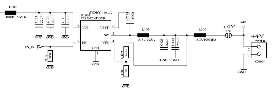
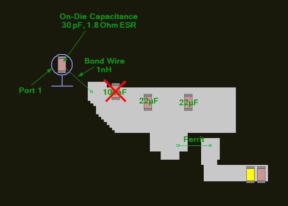
I have used the synchronous converter TPS563201 from TI. In addition, I usually decouple the converter at its input and output with ferrites. This attenuates noise but also makes the behavior more predictable as the influence of connected traces beyond the ferrites is negligible. The impedance at the input VIN is determined mainly by C111, C114 and C118 at frequencies above 100 kHz.
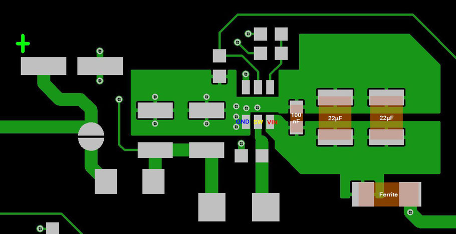
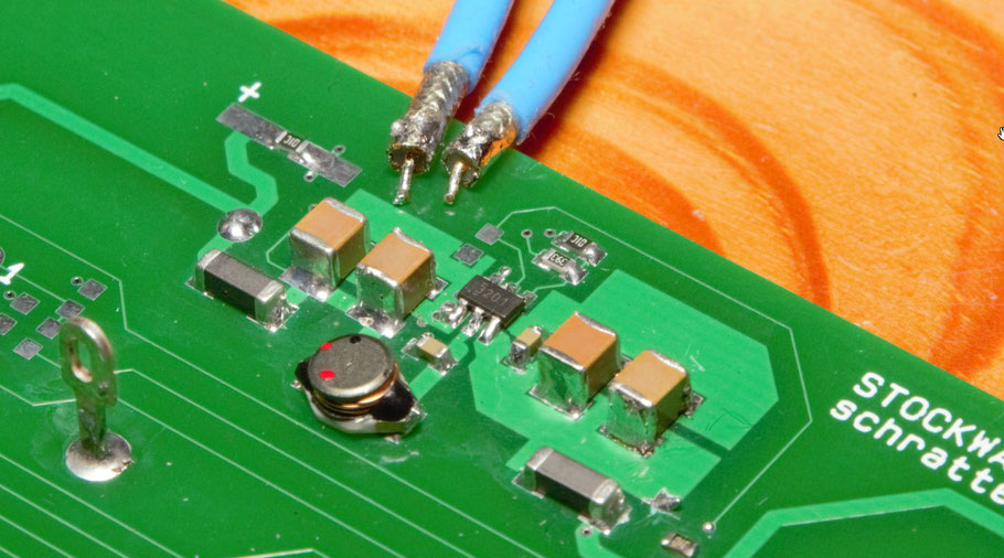
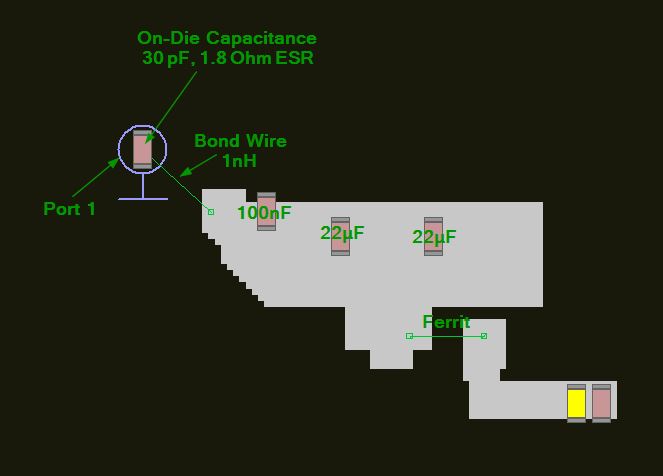
You can see the layout here. I have placed a 100 nF capacitor as close as possible at the input side of the converter. Two 22 µF caps are placed next. They add enough capacitance to compensate for the inductance of the ferrite at low frequencies. The bottom of the PCB is GND. The pinning of the converter IC makes the placement reasonably easy. There are not many alternatives.
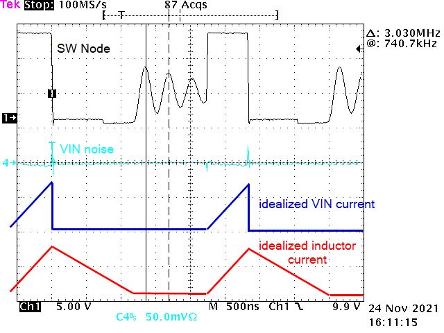
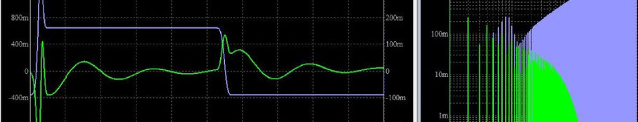
This is the waveform of the SW node at light loads in discontinuous conduction mode. Since the inductor current is zero when the High Side FET starts conducting, there is no fast current pulse at the input pins when the SW node raises to the supply voltage. A fast current slope is only present when the High Side FET is turned off. At the falling edge of the SW node, the current into VIN shows a fast falling edge, too. At this point the noise generated at the VIN pin is at its most. Immediately after the falling edge, the SW node is limited to a diode voltage drop below GND for a few ns before the synchronous FET is turned on bringing the voltage to nearly zero volts. The bottom FET is turned off after 700 ns which results in an increase of the voltage to -0.7 V again. When the inductor current reaches zero a damped oscillation is generated determined by parasitic elements. Since the High Side FET is off at this point, the oscillation is not present at the input side of the IC.
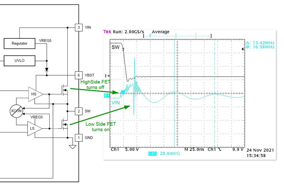
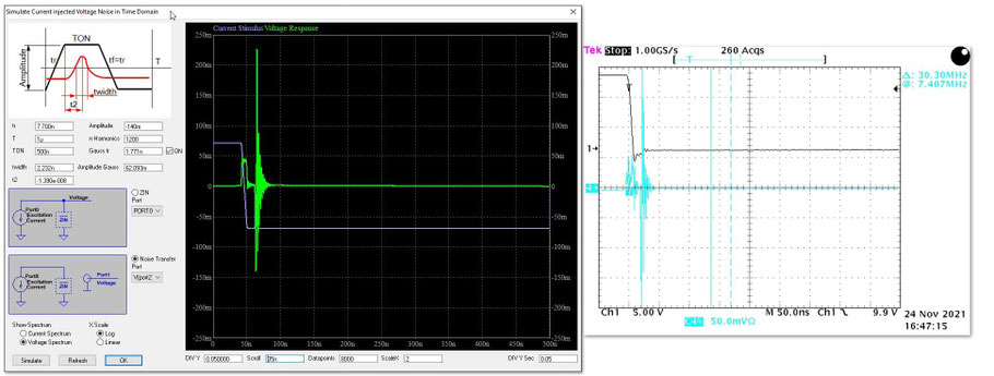
A zoomed in view shows the voltage at the VIN pin at the falling SW node edge. The voltage at the VIN pin starts to increase leading to an oscillation with about 13,42 Mhz. But the biggest spike appears 25 ns after the falling SW node edge. It is when the synchronous FET is turned on. The amplitude of this spike strongly depends on the VIN voltage level. I assume some kind of shoot through in the gate driving circuit.
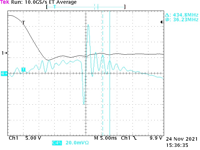
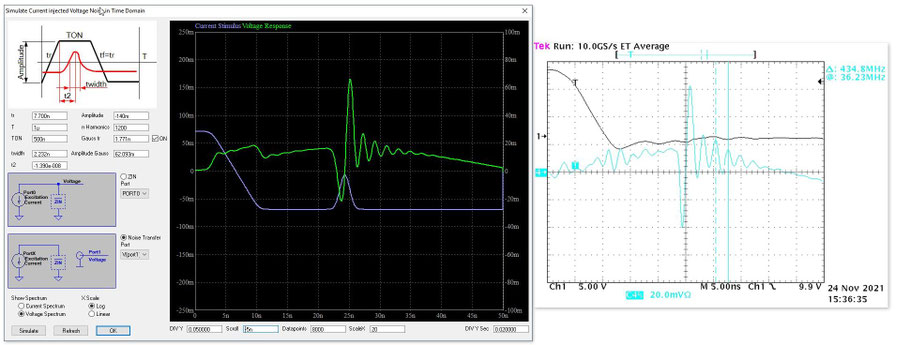
For this high frequency spike, the ringing frequency is about 434 MHz. The amplitude is 100 mV. The measurement is carried out with a semirigid cable directly soldered to the 100 nF capacitor. The oscilloscope terminates the cable into 50 Ohms and is set to AC coupling.
To fully understand why the ringing occurs at 13.42 Mhz and 434 Mhz the VIN node was simulated with the tool I have programmed in the past. I have made a measurement with a VNA and trimmed the values in the simulation to match the result with the measurement. For example, the value of the 100 nF capacitor was decreased to 42 nF. This is likely due to the voltage dependence of the dielectric material of the capacitor. Also, the converter IC itself creates an additional resonance due to its bond wire inductance and intrinsic capacitance of the integrated switching FETs. The value of this capacitance changes with VIN. This is a typical behavior for the capacitance of semiconductor junctions, since the junction width changes with voltage.
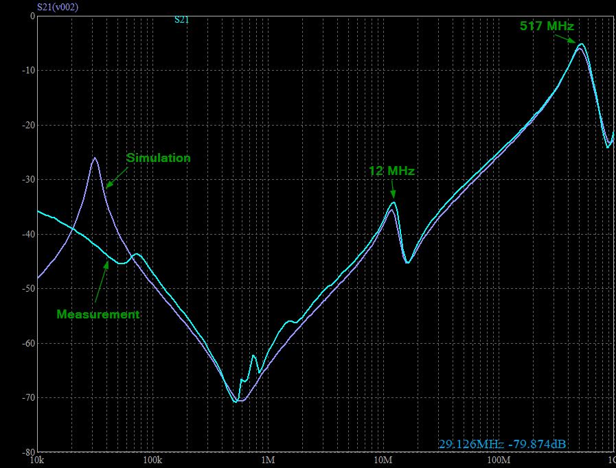
The diagram shows the simulation result compared to the measurement. For the measurement, the two ports of the VNA were soldered directly to the GND and VIN pins of the IC with a semirigid cable. The measurement of S21 is best suited to determine small impedance values, and could be converted to impedance by multiplying by 25 Ohm for a first approximation. The resulting simulation shows resonances at 12 Mhz and 517 Mhz. This confirms the measured ringing frequencies of the VIN voltage.
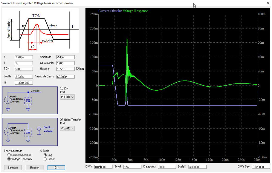
I have added the capability to perform simple time domain simulations with the tool. Here the simulated impedance is excited with a current source in the time domain. The purple waveform shows the current source waveform and the green waveform shows the resulting voltage noise. Again, I have tweaked the values of the current source so that the resulting voltage waveform matches the measured one. I can imitate a combination of a trapezoidal waveform and a Gaussian pulse in the time domain.
Next, I want to set up an experiment to show the importance of the 100 nF capacitor.
I have simulated the same scenario but without the 100 nF capacitor.
This results in an increase of noise voltage by about 400 % or 12 dB. It is interesting to note that the resonance at 13,42 Mhz has disappeared completely.
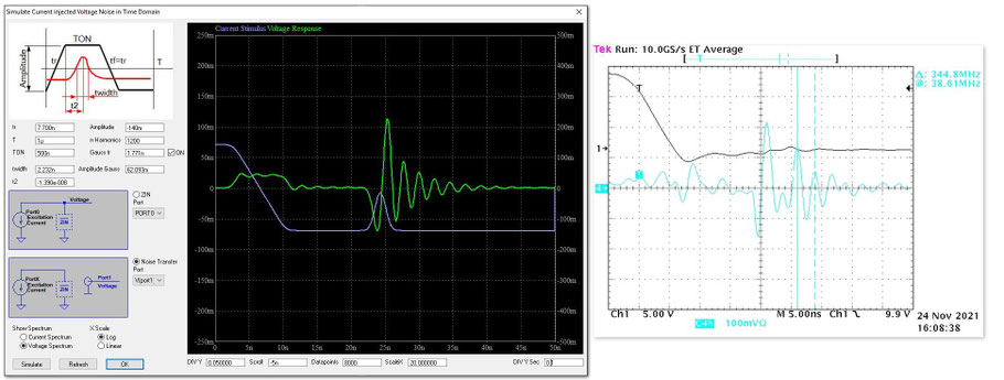
The ringing frequency of the high frequency spike has decreased slightly to 344 Mhz.
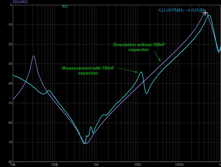
The simulated S21 parameters show that the resonance at 13,42 Mhz was created by the 100 nF capacitor. Also, the highest resonance frequency at 421 Mhz has decreased without the influence of the 100 nF capacitor. However, this simulation does not indicate the severe increase in noise voltage.

Another simulation could better show the rise of the noise voltage. Here the net is excited with an AC current source at the VIN pin. The resulting voltage at the position of the 100 nF capacitor is shown in the diagram. Now the increase of the noise voltage by 11 dB is better visible.
Write a comment