Ground bounce is often suspected to generate problems like EM radiation issues and measurement errors. In this context, fast digital lines are often mentioned to generate ground bounce on PCBs. The problem is that there is no common method to predict the level of ground bounce. A research often leads to the concept of partial inductance. Partial inductance is difficult for me to imagine, so I have decided to make some experiments on this topic. A very good paper can be found here https://www.academia.edu/3336105/Know_the_Theory_Of_Partial_Inductance_to_Control_Emissions.
Ground bounce is often explained as the voltage drop the signal current generates due to the inductive behavior of the ground plane. This was the starting point of my experiment. I wanted to measure the voltage drop on a ground plane excited by the return current of a microstrip signal. So far, so good.
At the same time, I heard that Ansys offers a free student version of its HFSS 3D-field solver. I really wanted to take advantage of this opportunity.
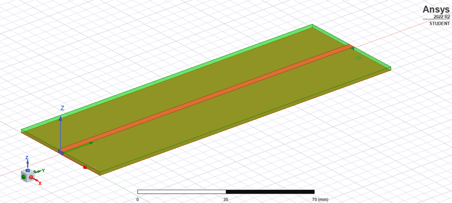
This is the microstrip line to be investigated. A simple copper track above a ground plane. The width of the line is 2,2 mm and the thickness of the FR-4 material is 1,2 mm.
What is tricky is how to measure / simulate the voltage drop of the ground for high frequencies.
Since with HF everything should be considered as a transmission line and common mode current is nothing else than the differential mode current of a higher order system, I decided to make the geometry of the ground plane itself like a microstrip line. Then I can make a short on one end and terminate the other end to measure the voltage with a VNA.
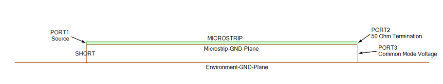
PORT1 will be connected to the microstip line. Here, the signal will be injected. The end of the microstrip line is terminated in PORT2. This can be a 50 Ohm termination resistor on a real board.
The Microstrip ground plane itself is shorted to a second, larger ground plane on the left side. If a common mode voltage is generated, it can be measured on the right side of the Microstrip ground plane. PORT3 is connected at this position.
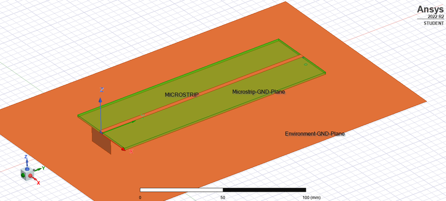
Here the 3D model is shown. You can see the PCB mounted above a second larger ground plane.
An equivalent circuit diagram in its simpliest form would look like this in SPICE:
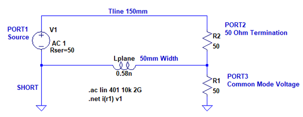
A sinusoidal signal is generated in a 50 Ohm source. Then the signal propagates along a 50-Ohm transmission line not modeled. The transmission line is terminated into a 50 Ohm resistor. The return current has to pass thru the inductive Microstrip ground plane. “Lplane” represents the partial inductance of the ground plane here.
Here a common mode voltage is generated, which can be measured at PORT3, which is terminated into 50 Ohm.
The result in form of the scattering parameter S21 is shown next:
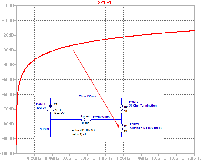
It shows the inductive behavior where the common mode voltage increases steadily with frequency.
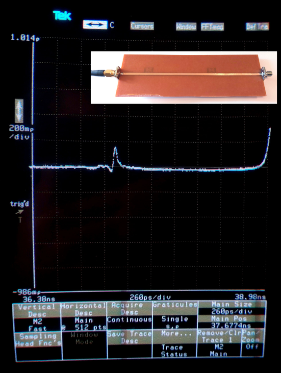
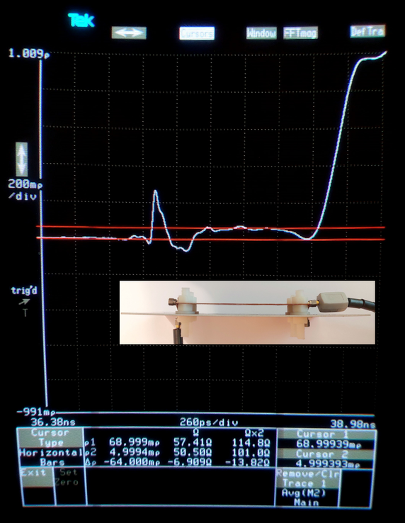
For validation a real model was built and measured with a VNA and a TDR. The L-value used in the spice simulation was extracted from the real measurements.
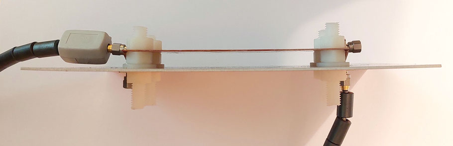
The model was built from raw single-sided copper-clad PCB laminate. SMA connectors are soldered to the microstrip line.
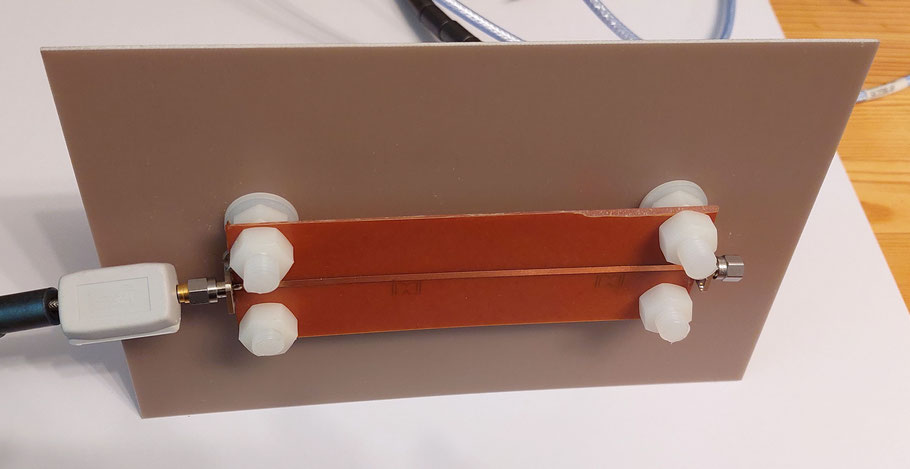
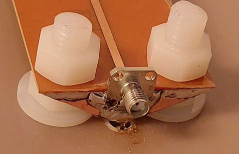
The ground plane was extended to additional SMA connectors on the bottom side to connect the ground plane of the microstrip line and the large ground where the PCB is mounted to with PVC threaded rods.
The side view of the model with attached cables for VNA measurements:
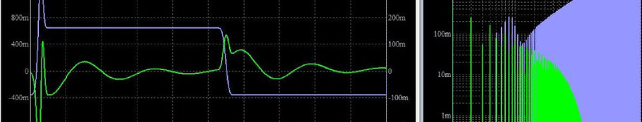
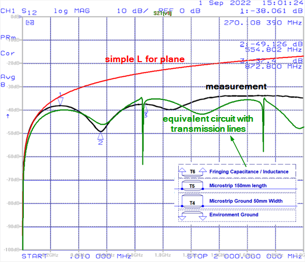
The measurement of the real model in comparision with the simple SPICE simulation:
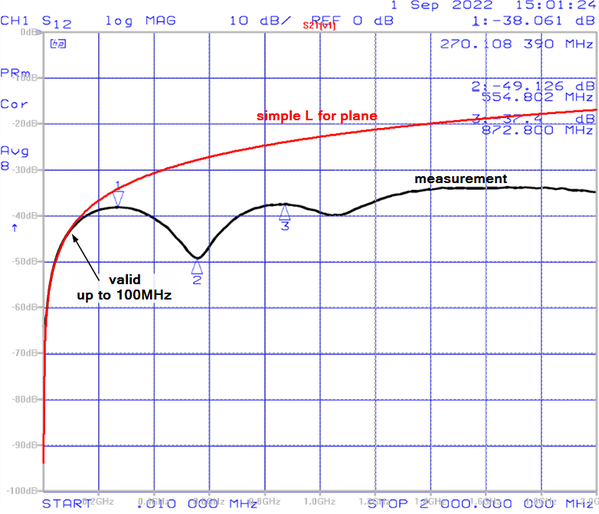
The equivalent circuit only gives a good match up to 100 Mhz. The measurement shows a first maximum at 270 Mhz followed by a resonance at 554 MHz.
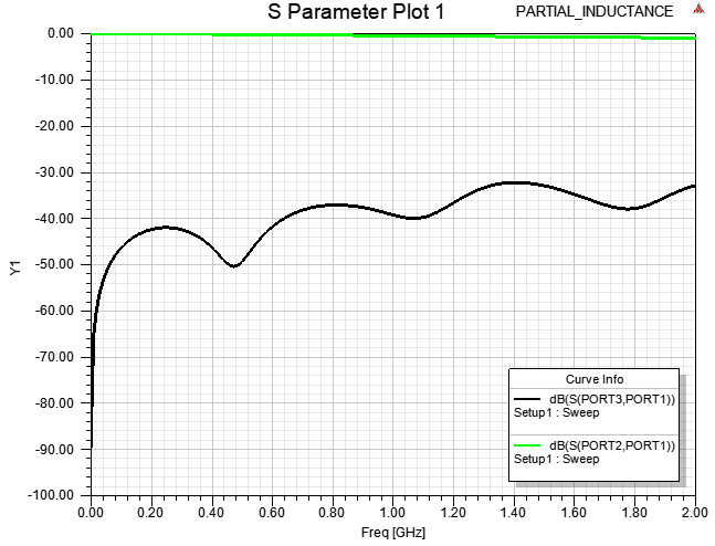
The simulation results in HFSS shows a much better match to the real behavior:
Next I want to show some results from the HFSS simulations.
With the 2D field solver the electrical field lines of the microstrip track can be displayed.
These are the field lines of the electric field when the voltage is at its maximum. They can be thought of to create the capacitance per unit length of the transmission line. In an ideal microstrip line, there are only field lines between the conductor and the ground plane.
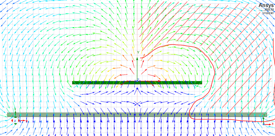
If we zoom out, we can see that there are additional field lines ending at the environment ground plane. This means there is additional capacitance between the microstrip track and the environment ground.
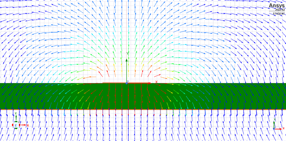
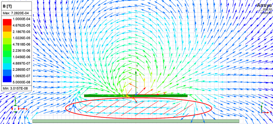
The same is true for magnetic field lines. With an ideal infinite ground plane there would not exist magnetic flux lines below the ground plane. The picture shows field lines below the microstrip ground plane. These flux lines wrapping around the ground planes are responsible for the partial inductance.
In my understanding the existence of the additional environment ground creates equal fields in between the ground planes and decreases the effective inductivity by a small amount.
I conclude that there is additional capacitance and something like inductance in parallel between the microstrip line and the large environment ground plane.
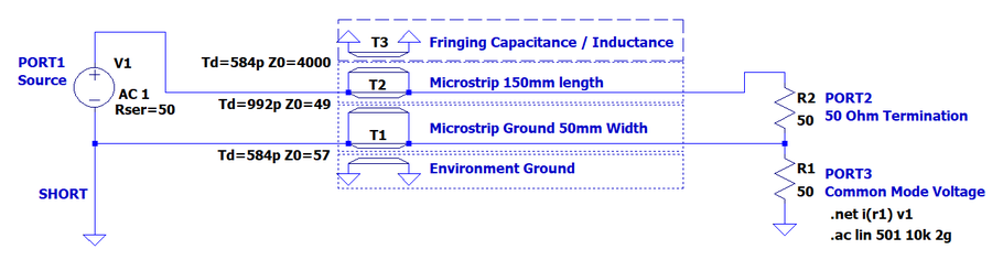
I have combined the information of the field solver in a new equivalent circuit.
T2 is the microstrip line on the PCB with a length of 150 mm. I used the result from the field solver of 49 Ω and the measured propagation delay from the TDR.
T1 represents the transmission line build up from the large environment ground plane and the ground plane on the underside of the PCB. The field solver calculates an impedance of 57 Ω and the TDR measurement showed a propagation delay of 584 ps.
Then comes the interesting part which is to model the extra capacitance between the microstrip trace on the PCB and the large ground plane on which the PCB is mounted. The propagation delay should be identical to T1, as most of the field lines are in free air. I have tuned the impedance value so that the simulation matches the measured result.
The result of this equivalent circuit gives a better match between simulation and measurement. And in my opinion, it better illustrates how common mode voltage is created.
For me the model gives a explanation of why the common mode voltage builds up in the microstrip ground plane. It is due to the additional capacitance / inductance that exists between the microstrip track and the environment. Which lead to extra current flowing in the environment ground plane. The arrangement between the housing and PCB ground then in turn determines which voltage is generated due to the currents.
Write a comment