Quick Start Guide
First Start
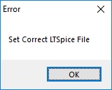
When you first start the program, you get a message to set the correct LTspice Path.
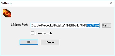
The path to the LTspice executeable must be entered here.
Create New Project
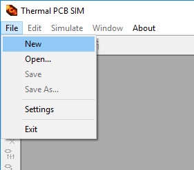
Open a new project.
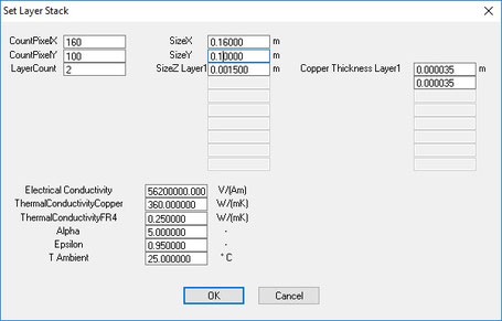
A diolog appears and you can enter the dimensions and pixel count. You can accept the default values.
Draw Copper
Two windows appear. One for editing and one for displaying the results.
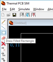
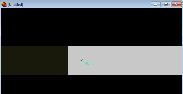
Now draw a rectangle by selecting the rectangle icon from the left toolbar.
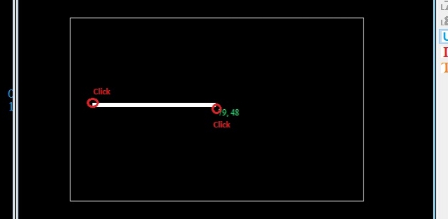
Draw a rectangle from the left to the middle by clicking the top left corner and bottom right corner. With default values each pixel will represent 1mm. This is our first conductor on the top side.
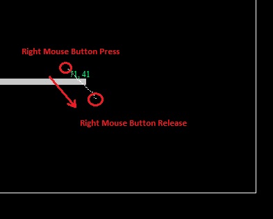
You can zoom in and out using the mouse wheel. You can also use the right mouse button. Press it and drag from top left to bottom right to zoom to that region. Release the mouse button.
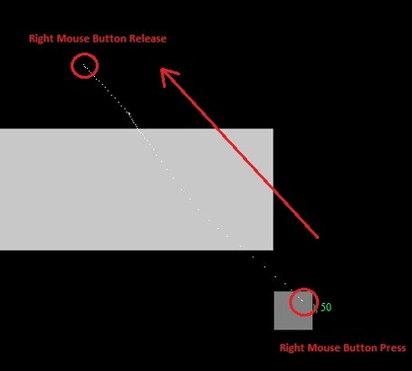
If you move the cursor from bottom rightto top left while pressing the right mouse button you can zoom out.
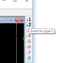
Switch to Layer 2 by pressing the "L2" button on the right toolbar.
Draw a second rectangle on Layer 2. You can make it wider or smaller as you like. They should overlap in the middle so you can add a Via in the next step.
Add Via
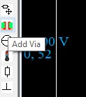
Select the Add Via Icon on the left toolbar.
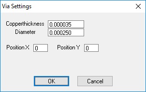
A Dialog appears. You can change Via Diameter and Copperthickness. All dimensions are in m.
Place the via in the area, where top and bottom copper overlap.
Add Current Source
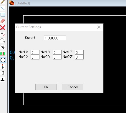
Select the icon for adding a current source on the left toolbar. A dialog appears. You can use default values.
Place the current source from the left to the right. We will change the layer in the next step.
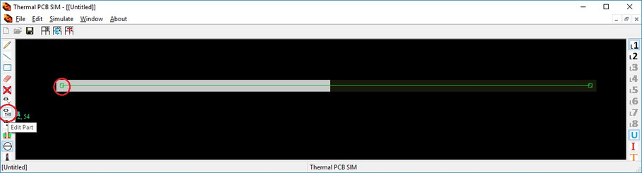
Select the "Edit Part" icon from the left toolbar and click on the current source in the edit area.
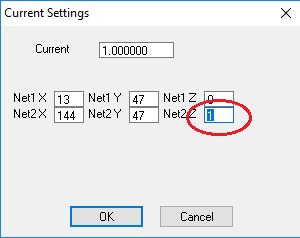
Now change the coordinates from "Net2 Z" from 0 to 1. This represents Layer 2 - sorry for the inconsistency :)
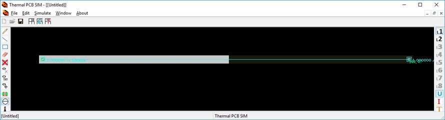
Add GND
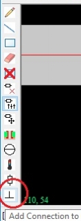
Select "Add Connection to GND"
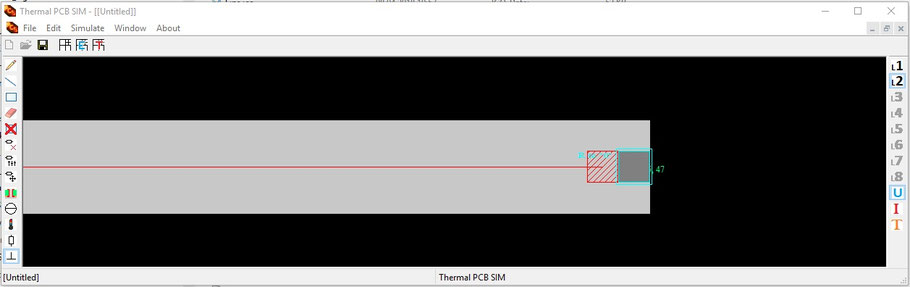
Place a GND connection at the right side of the conductor on Layer 2. You should always connect your conductor to GND somewhere.
Simulation
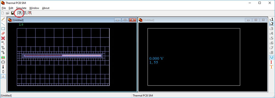
There are always three steps to simulate the project.
- First you have to create the mesh.

- Then simulate the board electrically
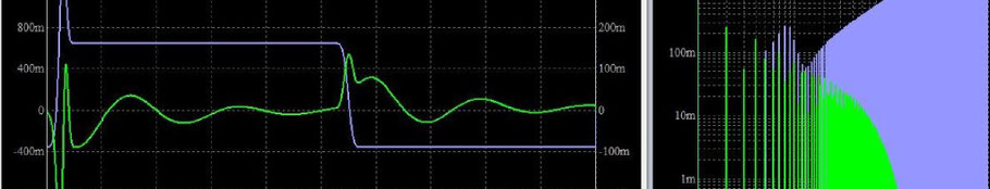
You will see a first result in the result window
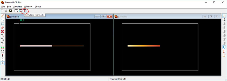
- Then you have to simulate the board thermally
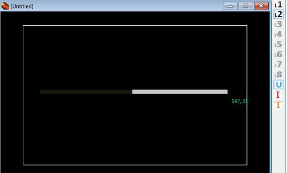
Showing Results
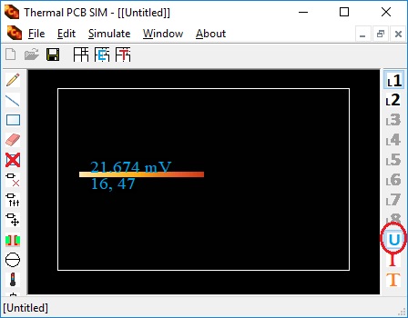
On the right side you can choose between voltage distribution "U" current density "I" and temperature "T".
With voltage distribution you can sense the voltage on the conductors in the result window.
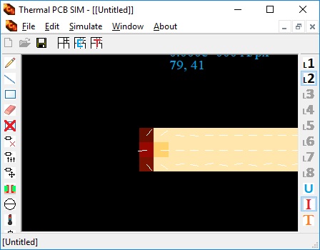
By clicking on "I" the current density is displayed. Also small lines indicate the direction of current flow.
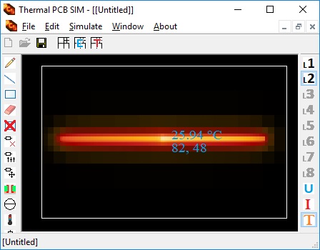
Finally by clicking on "T" the temperature rise will be displayed.